1. Development of comprehensive verification environments using UVM‑based methodologies to validate functionality across block‑level and SoC‑level designs
2. Creation of constrained‑random, directed, and coverage‑driven test suites ensuring thorough validation of digital, mixed‑signal, and high‑speed IP
3. Integration of assertions, functional coverage models, and scoreboards to accelerate bug detection and improve verification completeness
4. Collaboration with design, DFT, and firmware teams to ensure seamless bring‑up, debug, and validation from pre‑silicon simulation to post‑silicon characterization
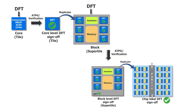
1. End‑to‑end DFT architecture development enabling robust test coverage across digital, analog, mixed‑signal, and memory subsystems
2.Implementation of scan insertion, compression, MBIST/LBIST, boundary scan, and test access mechanisms aligned with industry‑standard methodologies
3. Generation, verification, and optimization of ATPG and BIST patterns ensuring seamless bring‑up on ATE platforms and efficient transition to high‑volume manufacturing
4. Close collaboration with RTL, verification, and physical design teams to ensure test logic integration meets timing, area, and power constraints
1. Complete physical implementation flow from floorplanning to GDSII, ensuring timing‑driven, power‑optimized, and congestion‑free layouts for complex SoCs
2. Clock‑tree synthesis, routing optimization, IR‑drop mitigation, and EM/thermal reliability analysis for high‑performance and low‑power designs
3. Integration of DFT structures, memory macros, high‑speed interfaces, and analog blocks while maintaining physical integrity and manufacturability
4. Signoff using industry‑leading tools for STA, physical verification, parasitic extraction, and ECO closure to ensure first‑pass silicon success